Research
Research facilities and expertise
Our research expertise covers design, simulation, fabrication and measurement of photonic devices and systems. This includes numerical finite element modelng, rigorous theoretical analysis techniques, semiconductor microfabrication/nanofabrication and photonic device measurments. The School of Electronics operates a semiconductor cleanroom with standard wet benches, optical lithography equipment, thermal and sputter deposition systems and plasma etching tools for patterning silicon and other semiconductor materials. A host of measurement and analysis tools such as SEM, AFM, SNOM, Raman microscopy and ellipsometery plus a wide range of fixed and tunable laser sources are also available for device characterisation. Examples of our research activites are described below:
Integrated Photonics
Photonic Integrated Circuit (PIC) technology is a fast-growing sector of the optics industry and is estimated to command a market share of about £1B by 2022. Silicon and III-V material platforms are widely used for realising PICs but other materials are also being considered and developed.
For guiding and manipulating light signals on a photonic chip, an appropriate waveguiding platform with low losses is required in order to create efficient optical interconnects.For this purpose, a novel nanofabrication process is presented where silicon waveguides with record low losses are fabricated through a localized oxidation process, rather than the standard plasma etching step which creates rough sidewalls.
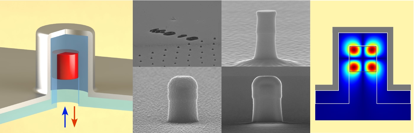
Active plasmonics and metallo-dielectrics
Metals offer a unique medium for guiding and manipulating light, owing to their abundant store of free electrons. This enables them to exhibit high optical reflectivity in conjunction with a negative permittivity which enables the propagation of optical waves (or plasmon polaritons) on their surface. However, they also exhibit high optical losses due to collisions between individual electrons. One method of compensating this loss is to incorporate an optical gain medium adjacent to the metal surface.
Another approach is to utilize reflective, rather than plasmonic optical modes. These modes can be designed to have lower losses due to less overlap with the metal layers. Using this approach the first example of a nanolaser with a 3D sub-wavelength cavity operating at room temperature has been demonstrated.